Streamline your KiCad projects with GitOps
Published on
I make a lot of PCBs - and some of them never actually get made (I have shiny object syndrome). Even so, streamlining a lot of the backend process makes designing them easier. I thought I would go over my workflow and how I design. This is pretty geared towards using KiCad, so YMMV if using another tool.
Making the Thing
So obviously the first step in my workflow is actually designing the thing - making the schematic, routing the PCB, and so on. I do keep a few things in mind to make my life easier later though - I have a column in my schematic BOM that is a direct part number for parts at my PCB assembly house, so it’s easier to upload the file and have it made later versus correlating them all when I go to order. Then once I’m done with the design (though, is any design ever really “done”?) I add it to my Git repo and push. I have a monorepo of all of my PCB designs (finished or not) that I just add it to. Once pushed, this triggers a workflow in GitLab to build the output files.
The Git Workflow
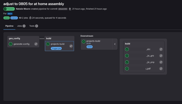
The CI job in GitLab was carefully designed to be as efficient as possible. To this end, the repo will be smart and only run jobs for boards that have been changed. The workflow will kick off a first job to calculate diffs from HEAD to HEAD~1 and only run jobs for projects that have been modified in this push. For example, if my repo structure looks like:
pcbs /
|- proj_1 /
|-- proj_1.kicad_pro
|-- (...)
|- proj_2 /
|-- proj_2.kicad_pro
|-- (...)
|- proj_3 /
|-- proj_3.kicad_pro
|-- (...)
|- (...)
And these are the only changed files in the current push:
pcbs /
|- proj_1 /
|-- proj_1.kicad_sch
|- proj_2 /
|-- proj_2.kicad_pcb
Then only proj_1 and proj_2 will be built. This is obviously nice for my CI runners (or saving CI minutes on GitHub), but after living with this for a while, it has the unfortunate side effect of there not being an easy way to manually rebuild a project. The easiest way I’ve found to force a rebuild is to create a dummy file in a project directory that you want to force a rebuild for and pushing that. That’s enough to trigger a rebuild for the whole project even if you didn’t touch the KiCad files.
Once the modified projects are calculated, a child workflow file is created for just the modified projects, then saved as an artifact and sent to the CI coordinator for execution.
The workflow leverages the KiCad CLI Docker image quite a bit, which is really the backbone of the whole project. If you have another environment, e.g. Eagle, Altium, etc; your mileage may vary for what sort of command-line tools you have to automatically plot your PCBs.
Variables
In the workflow there are two main variables you can define in text files. One is the layer count - currently I don’t have a good way of detecting how many layers are in a PCB project, so by default the workflow will assume 2 layers, and if it finds a LAYERS file in the root of your project it will read the contents of that and use that as a layer count - so for example if I had a 4-layer PCB, I would just make a LAYERS file that only has the number 4 in it to denote that this project is a 4-layer PCB.
Second is ERC/DRC enforcement. This is discussed a bit later, but you can selectively enable rule enforcement for a particular project whereby the workflow will fail out if there are any errors in your design (versus just writing the errors out normally). To enable enforcement, all that’s needed is to create a blank file named ENFORCE_RULES in the root of your project.
PDF Artifact
The first job that runs is a PDF export of both the schematic and PCB. These are mostly useful for reference. There isn’t much going on here!
ERC/ERC Testing
As mentioned earlier, one step of the workflow is ERC/DRC rule testing. Failing a rule check can be either fatal (e.g. causes the workflow to not progress) or soft (e.g. the workflow will continue even if there are grave errors in your design). This is decided by the presence of the ENFORCE_RULES file. Currently all tests specified in the project are run, and warnings and errors are both logged.
Gerber Artifact
Since every PCB house is different, settings here will vary based on what your PCB house wants. After rule checking, a set of Gerber files will be made for the project using consistent export settings (i.e. it doesn’t care what you have set in KiCad, it will export how it pleases). Currently I only have settings for one PCB house in the workflow but it’s not too hard to have multiple output formats for different manufacturers. As part of the current export it will plot all layers (taking into account the layer count specified in the layer file), create a drill file and drill map.
Pick-and-Place Artifact
As mentioned above, every PCB house is different, so settings here will differ a bit. At this stage the workflow will first export a BOM containing the part designator and part number. Then it will export a component location file for the pick and place machine to know where to place SMD components. This has to be touched up a bit for my PCB house, so there’s a bit of post-processing.
Kiri Diff Artifact
This is a work-in-progress, but by using Kiri you can create a visual diff of your schematic and PCB. I’m working on implementing this into the workflow.
Source Code
I am working on a few enhancements and general cleanup, then I will post a link to my Github with the workflow to use. Stay tuned!